GlobalFoundries said on October 14 that it was selected to operate two planned semiconductor fabs in Malta, New York, under a U.S.-Japan investment initiative. The company announcement values the GlobalFoundries fab plan at up to $21 billion if both facilities move ahead.
GlobalFoundries fab plan sets a 2029 target
Japan would provide investment capital while GlobalFoundries supplies the technology and operates the facilities. The first fab is expected to begin production in 2029, subject to final agreements, regulatory reviews and construction milestones.
The second facility remains conditional on additional investment. If completed, the two fabs would add substantial domestic capacity for technologies used across automotive, communications, industrial and defense applications.
The scale also highlights the capital intensity of chip manufacturing. Investors comparing semiconductor businesses often use revenue multiples alongside growth and margin expectations, making the mechanics in this price-to-sales ratio guide relevant when evaluating expansion plans.
Funding combines U.S. and Japanese support
The initiative could provide up to $21 billion across the two facilities and associated activity. GlobalFoundries said the United States and Japan developed the plan as part of a strategic technology partnership aimed at strengthening semiconductor supply chains.
The U.S. Commerce Department also amended GlobalFoundries’ existing CHIPS award. The revision reallocates $955 million toward silicon photonics, silicon-germanium and advanced packaging work in New York and Vermont. Commerce would receive an equity position equal to about 4% of GlobalFoundries under the amended arrangement.
Advanced packaging and specialty chips are increasingly important to AI infrastructure. That connection is visible in new model launches such as Google’s Gemini 4 Argon rollout, which depends on continuing investment across computing, networking and power.
Capacity and execution will shape the market impact
Each planned fab would have annual capacity of approximately 900,000 300-millimeter wafers at full operation. The first facility’s 2029 target means the investment will affect supply gradually rather than deliver an immediate increase.
Construction schedules, equipment availability and customer commitments will determine how quickly GlobalFoundries can convert the project into revenue. The company will also need to manage working capital as it scales, an issue outlined in Fusion Market News’ cash conversion cycle explainer.
The announcement does not provide a time series suitable for an original market chart. Its core figures are forward-looking project totals and capacity targets, so the article describes the sourced milestones directly rather than presenting an artificial trend.
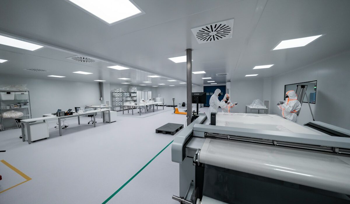
Featured image: Semiconductor cleanroom by TECNIC Bioprocess Solutions via Unsplash.

Elsy kanana
Elsy Kanana is a financial and cryptocurrency journalist at FusionMarketNews, covering digital assets, blockchain technology, financial markets, and emerging fintech trends. Her reporting focuses on market movements, regulatory developments, and on-chain analytics, delivering clear, data-driven insights to readers worldwide.